

AI MMW PCB Testing Station
AI MMW PCB testing station:
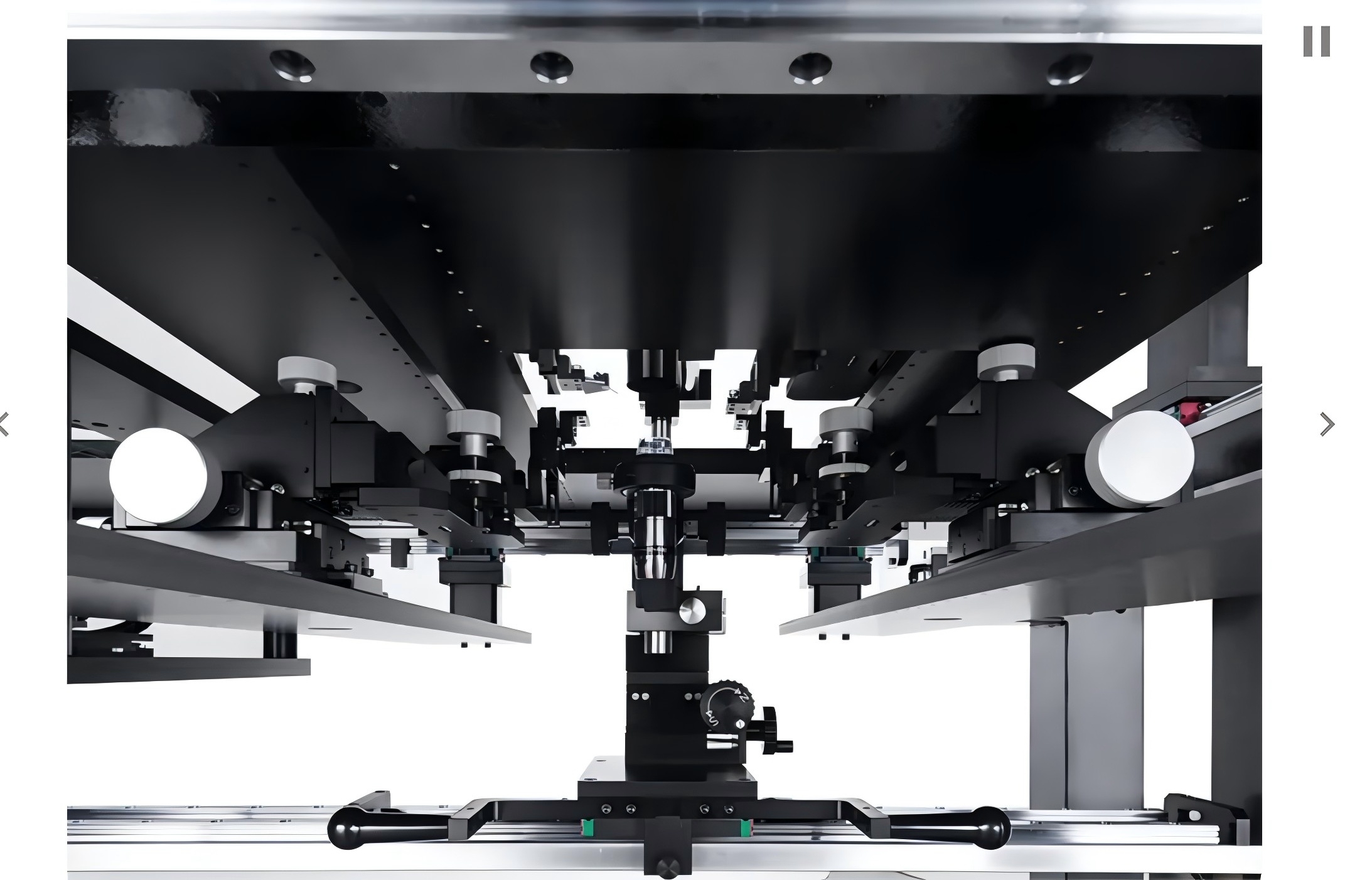
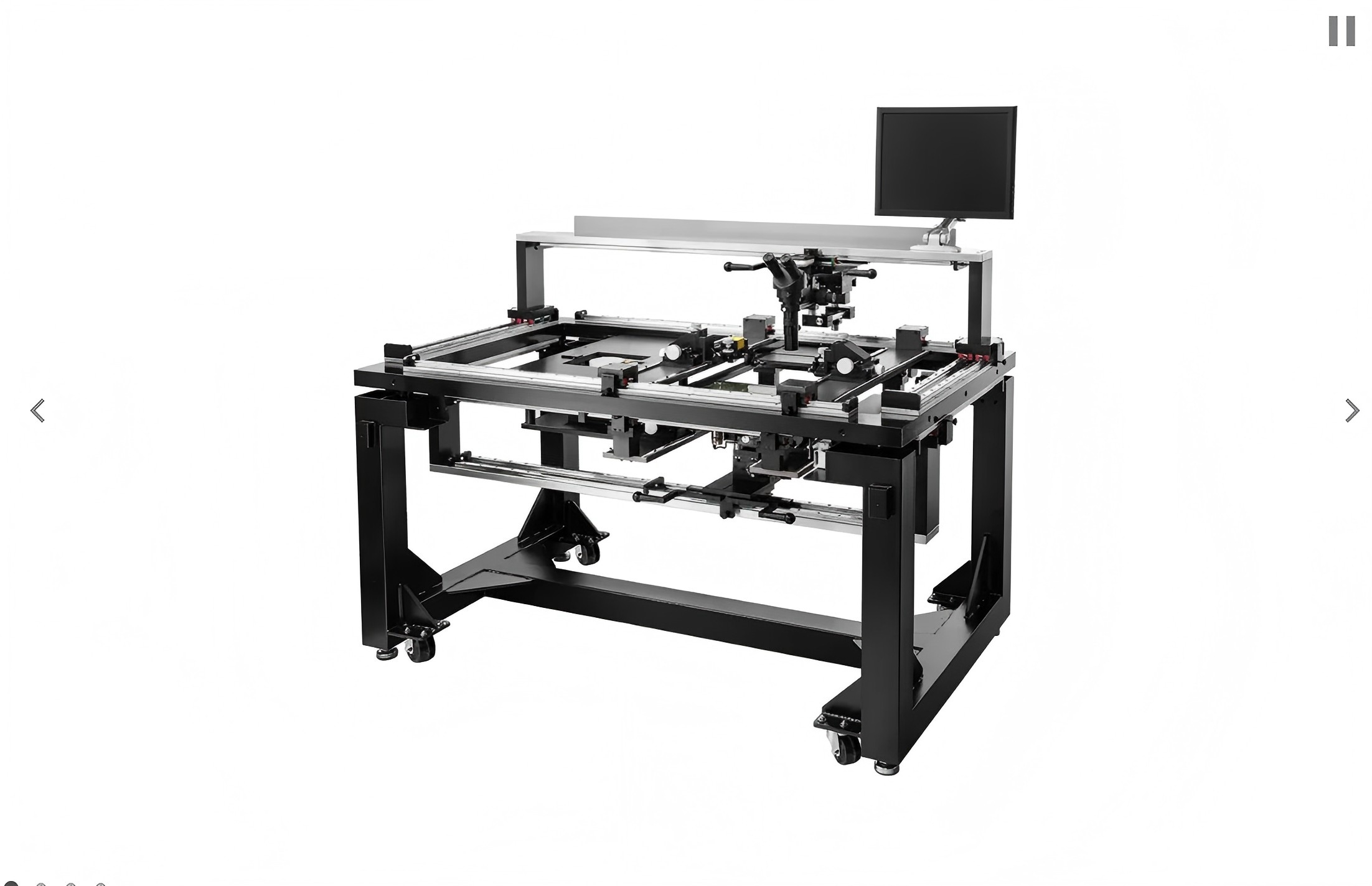
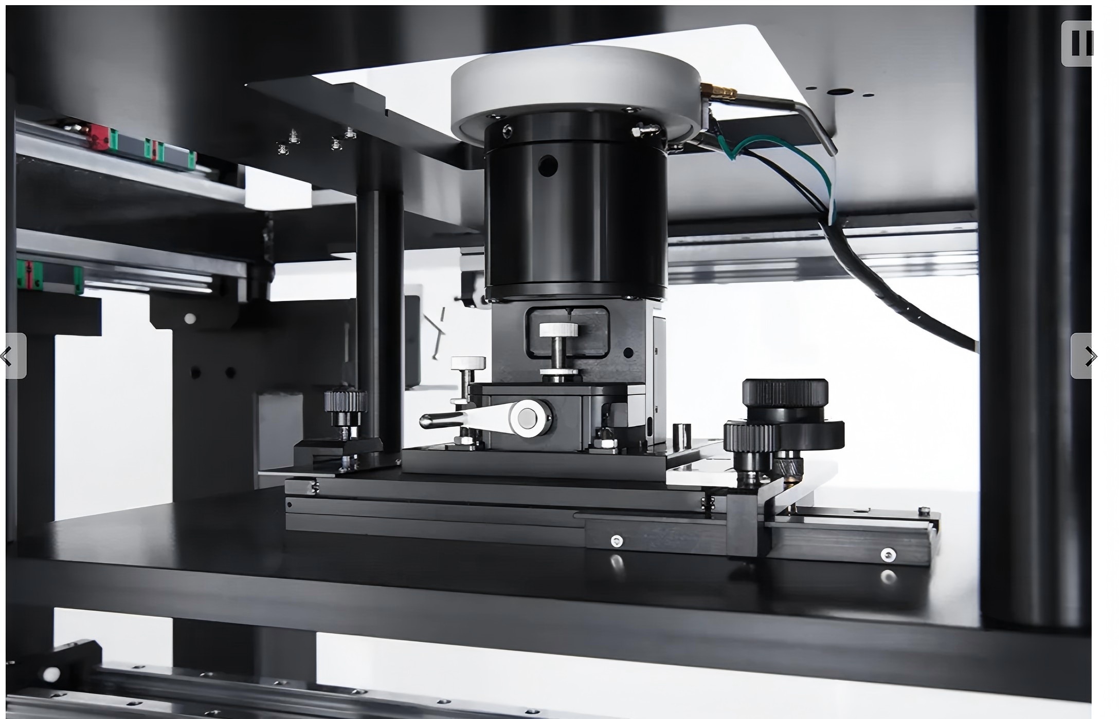
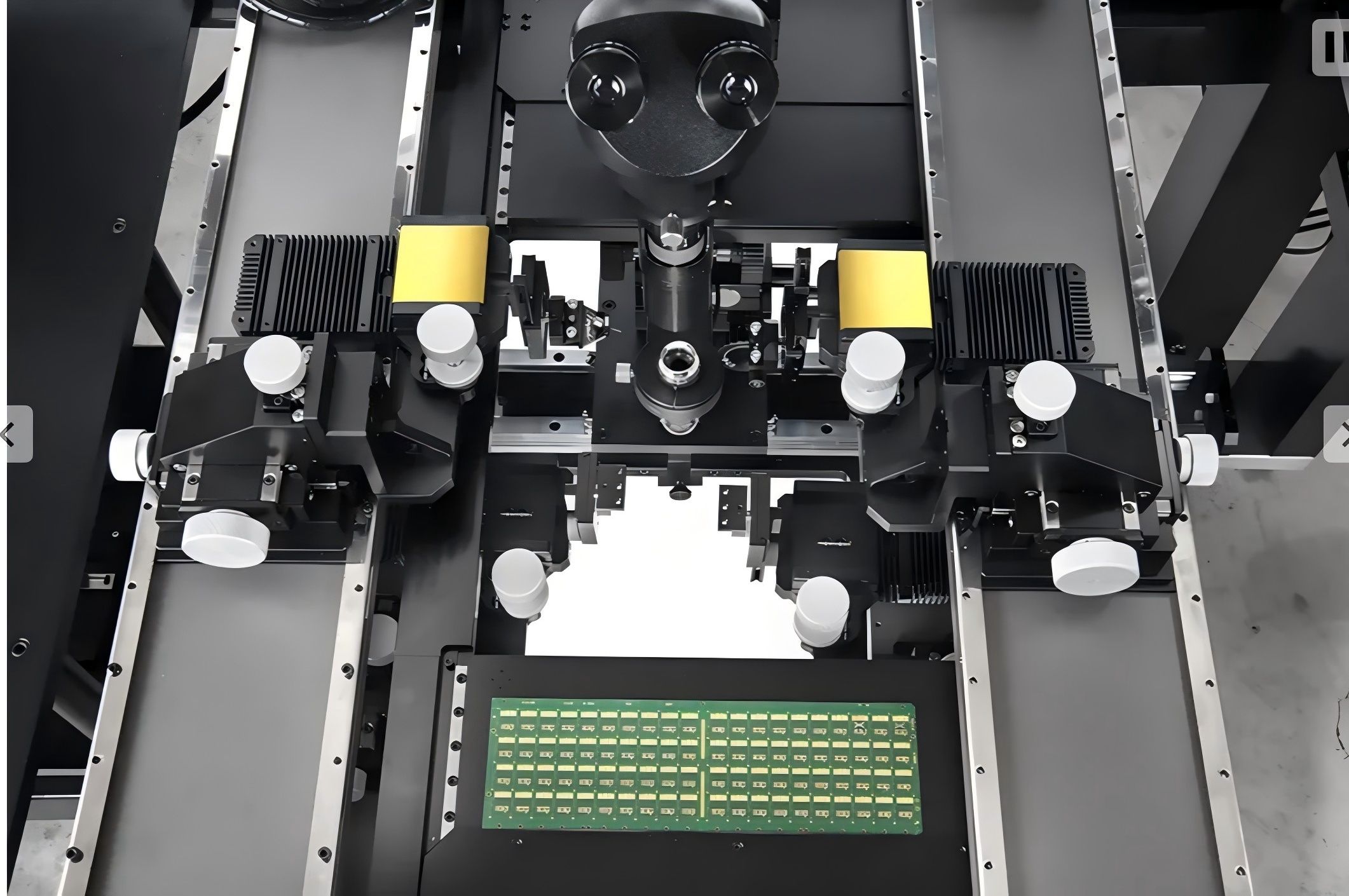
Everbeing's specially designed single/double-sided PCB test station for the world's leading AI PCB manufacturers contributes to the global AI revolution. Product test PCB size: Standard: 900mmX600mm (customizable according to customer requirements). The test station can provide single-sided PCB testing and also customize double-sided PCB test stations for customers. Equipped with Everbeing's unique high-performance air-bearing shock-resistant table, it provides a stable platform for high-frequency/high-speed signal testing. The display bracket and omnidirectional joint installed at any position facilitate users' observation of needle insertion and electrical performance parameters. Different millimeter-wave probe holders can be provided according to customer needs for testing signals. All RF and millimeter-wave probe brackets have international standard mounting holes, compatible with probes from all brands. High-quality microscopes and 4K high-definition digital cameras are provided according to customer test sample attributes or customer testing requirements. A PCB loading machine can also be provided for customers.
Application and Features of Test Stations:
1) AI Chip PCB Test Station (Highest Frequency Band: 325GHz), PCB Maximum Size (900mmWX800mmD) and Thickness: 60mm;
2) LEO Antenna Array Chip PCB Test Station (Highest Frequency Band: 500GHz) for Near-Field and Far-Field Testing;
3) New Smart Car Antenna Array Chip PCB Test Station (Highest Frequency Band: 500GHz) for Near-Field and Far-Field Testing;
4) Double-Sided Test Station (Needles Can Penetrate Both Top and Bottom Surfaces);
5) Maintenance and Upgrade of PCB Test Stations;
6) Millimeter-Wave Dual-Layer Four-Way Probe Station Compatible with Any Brand of Frequency Doubling Modules.
Everbeing specializes in Providing Customized Services. We look forward to your inquiry!